Publication
Electrostatically-induced strain of graphene on GaN nanorods |
Kierdaszuk J., Bożek R., Stefaniuk T., Możdżyńnska E., Piętak-Jurczak K., Złotnik S., Zubialevich V., Przewłoka A., Krajewska A., Kaszub W., Gryglas-Borysiewicz M., Wysmołek A., Binder J., Drabińska A. |
Applied Surface Science644, 2024, art. 158812, 10.1016/j.apsusc.2023.158812 |
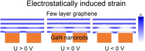
Few-layer graphene deposited on semiconductor nanorods separated by undoped spacers has been studied in perspective for the fabrication of stable nanoresonators. We show that an applied bias between the graphene layer and the nanorod substrate affects the graphene electrode in two ways: 1) by a change of the carrier concentration in graphene and 2) by inducing strain, as demonstrated by the Raman spectroscopy. The capacitance of the investigated structures scales with the area of graphene in contact with the nanorods. Due to the reduced contact surface, the efficiency of graphene gating is one order of magnitude lower than for a comparable structure without nanorods. The shift of graphene Raman modes observed under bias clearly shows the presence of electrostatically-induced strain and only a weak modification of carrier concentration, both independent of number of graphene layers. A higher impact of bias on strain was observed for samples with a larger contact area between the graphene and the nanorods which shows perspective for the construction of sensors and nanoresonator devices.